Working circuit of a signal generator on a microcontroller. Dendy is a generator of test television signals. A new version. Scheme, description. Description of CTC mode
As long as I have been working in electronics, I have always wanted to have a signal generator of various shapes. Recently I needed to obtain a sine wave signal using digital methods, and I decided that I would make myself a good generator! As a result, I made a simple but functional signal generator that can generate: square wave, triangle, sine, noise and sawtooth signals. The maximum generated frequency is 60kHz (kilohertz). So far, in this firmware, the frequency can only be set when generating a square wave; for other signals, only a delay in microseconds can be set. The basis of the device is the ATtiny2313 AVR microcontroller, the signal is generated using an 8-bit digital-to-analog converter (DAC), frequency, signal or delay data is displayed on an 8x2 LCD indicator. Here's the actual schematic diagram:
For assembly you will need parts:
1. Attiny2313 microcontroller - 1 pc.
2. LCD indicator WH0802 or HD44780 compatible - 1 pc.
3. LM324 chip - 1 pc.
4. Tact buttons without fixation - 3 pcs.
5. Resistor 10 kOhm - 1 pc.
6. Resistor 300 Ohm - 1 pc.
7. Resistor 2 kOhm - 8 pcs.
8. Resistor 1 kOhm - 9 pcs.
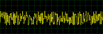
The DAC is assembled using resistors and connected directly to port B of the microcontroller, the signal after the DAC is amplified using an LM324 operational amplifier. I used the LCD indicator WH0802 with a compatible controller, this LCD has 2 lines of 8 acquaintances each. It is essential to use any LCD indicator with a compatible controller with HD44780. The Attiny2313 microcontroller can be used with any letter indices, in any package. You can use any tact buttons, without fixing them. The "Select" button selects the type of generated signal. The "Plus" and "Minus" buttons set the frequency or delay. When you turn on the device, it immediately begins to generate a signal, by default it is a square wave. Supply voltage: 5 volts. Here are the oscillograms of the signals generated by the generator:


I assembled my signal generator in a ZIV plastic case, and this is what happened:

First tests with a homemade oscilloscope:

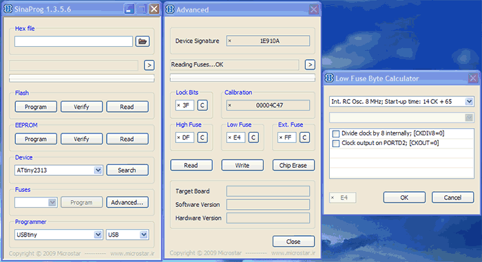
I assembled the circuit on a printed circuit board made using , a drawing of the printed circuit board can be found in the files for the article. On the board I used parts in SMD packages, with the only exception being the LM324 chip, which is used in a DIP package. I wrote the firmware for the device in the BASCOM-AVR environment, the source code is attached. Also attached is a device project in the program. By the way, after flashing the firmware, do not forget to set the following fuse bits (for the SinaProg program):
List of radioelements
| Designation | Type | Denomination | Quantity | Note | Shop | My notepad |
|---|---|---|---|---|---|---|
| U1 | MK AVR 8-bit | ATtiny2313 | 1 | To notepad | ||
| U2 | Operational amplifier | LM324 | 1 | To notepad | ||
| R1-R8 | Resistor | 2 kOhm | 8 | To notepad | ||
| R9-R16, R18 | Resistor | 1 kOhm | 9 | To notepad | ||
| R17 | Resistor | 10 kOhm | 1 | To notepad | ||
| R19 | Resistor | 300 Ohm | 1 | To notepad | ||
| BTN1-BTN3 | Button | Without fixation | 3 |
The timer generates time intervals of a given duration. Counter 1 counts these pulses and, if necessary, changes the time intervals generated by the timer. Counter 2 counts the required number of pulses and, having counted to the specified value, stops the timer.
Device operation algorithm
Timer T1 generates time intervals of a given duration; at the end of the interval, it generates an interrupt in which its values are updated. Thus, it is possible to generate any sequence of pulses with any parameters (period, duration, duty cycle).
The interrupt routine begins by checking whether this is the last pulse; if it is the last, the timer stops. If not the latter, a check is made to determine whether it is an impulse or a pause between impulses (impulse duration - 2500 μs, pause duration - 7500 μs), thus, the time intervals of the impulse and pause are formed alternately.

Description of CTC mode
Match timer reset mode (CTC)

Rice. 1. Block diagram of T0
In CTC mode (WGM01, WGM00 = 0b10), the OCR0 register is used to set the counter resolution. If CTC mode is set and the counter value (TCNT0) matches the value of the OCR0 register, the counter is reset to zero (TCNT0=0). Thus, OCR0A specifies the top count of the counter, and, consequently, its resolution. This mode provides a wider range of adjustment of the frequency of generated rectangular pulses.
In timer reset on match mode (WGMn3-0 = 0b0100 or 0b1100), the timer count limits are set by the OCR0A register. In CTC mode, the counter (TCNT0) is reset if its value matches the value of the OCR0A register. In this mode, it is possible to adjust the frequency of generated rectangular pulses. The timing diagram of the timer operation in CTC mode is shown in Figure 1. The counter (TCNTn) increments its state until a match occurs with the value OCR0A, and then the counter (TCNT0) is reset.

Rice. 2 Timing diagrams of the STS mode
In addition to the reset, an interrupt can be generated using the OCF0A flags corresponding to the registers used to set the upper count limit. If the interrupt is enabled, then the interrupt routine can be used to update the upper count limit.
To generate a signal in CTC mode, the OC0A output can be used to change the logic level on each match by setting the switching mode (COM0A1, COMA0 = 0b01). The value OC0A will be present on a port pin only if that pin is set to output direction. The maximum frequency of the generated signal is fOC0 = fclk_I/O/2 if OCRnA = 0x0000. For other OCRn values, the frequency of the generated signal can be determined by the formula:

where the variable N specifies the prescaler factor (1, 8, 32, 64, 128, 256 or 1024).
Program
Include"m16def.inc"
rjmp RESET ; ResetHandler
reti; IRQ0 Handler
reti;;rjmp EXT_INT1 ;IRQ1 Handler
reti;reti;jmp ;TIM2_COMP; Timer2 Compare Handler
reti;;reti;jmp ;TIM2_OVF; Timer2 Overflow Handler
reti; ;reti;jmp;TIM1_CAPT ; Timer1 Capture Handler
jmp TIM1_COMPA ; Timer1CompareA Handler
reti;reti;jmp;TIM1_COMPB ; Timer1 CompareB Handler
reti;reti;jmp ;TIM1_OVF; Timer1 Overflow Handler
reti;;reti;jmp ;TIM0_OVF; Timer0 Overflow Handler
reti;;reti;jmp ;SPI_STC; SPI Transfer Complete Handler
reti;;reti;jmp;USART_RXC ; USART RX Complete Handler
reti;;reti;jmp;USART_UDRE ; UDR Empty Handler
reti;reti;jmp ;USART_TXC; USART TX Complete Handler
reti;reti;jmp ;ADC ; ADCConversion Complete Handler
reti;reti;jmp ;EE_RDY ;EEPROM Ready Handler
reti;reti;jmp ;ANA_COMP; Analog Comparator Handler
reti;reti;jmp ;TWSI ;Two-wire Serial Interface Handler
reti;reti;jmp ;EXT_INT2; IRQ2 Handler
reti; Timer0 CompareHandler
reti;reti;jmp SPM_RDY ;Store Program Memory Ready Handler
ldi r16,high(2500)
ldi r16,low(2500)
ldir16,(1< ldir16,(1< ldir16,(1< ldi r16,high(RAMEND) ldi r16,low(RAMEND) out SPL,r16 ; sei ; main: ; ldi r16,high(2500) ldi r16,low(2500) ldi r16,high(7500) ldi r16,low(7500) After starting the microcontroller, the initialization procedure (RESET) occurs, in this subroutine sequentially: I/O ports are configured (port D is configured for output) The operation of timer T1 is configured: Loads the number (2500) into the comparison register Pin OC1A is configured to “flip” the level when the counting register and comparison register (OCR1A) match Sets the operating mode (reset by coincidence) and the clock source (no prescaler, from the system clock) The T1 coincidence interrupt is enabled The stack is initialized (the top of the stack is configured) Interrupts are enabled. This completes the controller initialization. Next, the program counter “goes” into the main loop. When an interrupt occurs, the interrupt handling subroutine TIM1_COMPA is launched, it begins with an increase in the number of interrupts (a sequence of eight pulses is given, and this is 16 “level flips”), the interrupt number is compared with 16, and, if equal, the out_pulse subroutine is launched. The timer is stopped in it (by resetting the control registers of the microcontroller). If the number of interrupts is less than 16, the program continues further. The breq pulse flag is checked and, if set, the pulse subroutine is run, which updates the comparison register (loading the number 7500) and resets the flag. Thus, based on the presence of the flag, the numbers 2500 and 7500 are loaded one by one, and a sequence with a duty cycle of 4 (as specified) is formed at the OC1A pin. The generator is designed to evaluate the quality of operation and configure color and black-and-white TVs. Of course, on LCD TVs there is no need to adjust color purity and reduce beams, but sometimes you may just need to check the TV’s performance. The proposed TV signal generator produces a complete television signal of the SECAM system (and with an additional encoder - also PAL), in which the relative arrangement of synchronizing and blanking pulses of lines and fields, equalizing pulses, components of the color synchronization signal are as close as possible to the requirements of the standard. Unlike most amateur TEST TV designs, the generator generates an interlaced raster with a number of lines of 625. The frame rate is exactly 50 Hz. The device provides color synchronization both across fields and lines, which allows you to configure color modules of any modification. The principle of operation of the television signal generator is to sequentially enumerate the addresses of the ROM in which the information displayed on the screen is programmed. This makes it possible to obtain various test images using relatively simple means. The diagram of the main board of the TV signal generator is shown in the figure. Each line of the television raster is divided into 64 familiar locations, in any of which a sync pulse level, black level, 8 gradations of white brightness or a white point can be formed. A 3900, 4250, 4406, or 4756 kHz color subcarrier can be superimposed on the luminance signal. To display one line, 64 bytes are required in DD5 ROM of type K573RF5, K573RF2 or 2716, which are selected by the six low-order bits of the address. DD6 K573RF4, 2764 or 27128 records information about which line is being generated at the moment. This is determined by digits 0...4. If digit 5 is programmed, clarity lines are entered into the corresponding familiar place. Bit 7 is used to limit the conversion factor DD1...DD4 to 625. Each television frame occupies 1 kbyte. In the original version, the television signal generator can generate the following test signals: Those interested can create their own image. Read the detailed description for how to do this. The design and setup procedure for this TV signal generator are also described there. The generator is connected to the antenna input of the TV, operating on the first or second television channel. By receiving various test images on the screen, you can converge the rays of a color picture tube, achieve color purity and white balance, correct geometric distortions, raster sizes and alignment, adjust focus, etc. The device generates a black and white field, six and twelve vertical stripes with gradations of brightness, vertical and horizontal alternating stripes and lines, as well as checkerboard and grid fields and many other combinations, including possible signal inversion. For the purpose of simplification, the generator generates a line-by-line raster with the number of lines 315. The frame rate is 49.6 Hz. The schematic diagram of the generator is shown in the figure. It consists of a reference frequency quartz oscillator (DD5.1, DD5.2), a television signal shaper (DD1 - DD4, DD5.3, DD5.4, DD6, DD7), an addition device (VD5 - VD7, R17 - R19) and RF generator (VT1). The quartz oscillator produces pulses with a repetition rate of 4 MHz. As a result of its division at output 15 of the VD2 counter, a pulse of 0.1 μs is generated for every 16th input pulse, generating signals with a frequency of 250 Hz. creates vertical lines on the screen. It goes to switch SB5. Counter D1 divides the repetition frequency of this sequence to lowercase (15625 Hz), at output 1 we receive a signal of vertical stripes, which goes to switch SB4.1. Resistors R2 - R5 convert the binary code signals at outputs 1, 2, 3, 4 of the DD1 counter into a stepwise changing voltage in brightness gradations. Horizontal damping and synchronizing pulses with a repetition period of 64 μs. are formed by triggers of the D3 chip. Before the pulse appears at input R, trigger DD3.1 is in the single state. A pulse arriving at input R sets it to the zero state, which corresponds to the beginning of the formation of a horizontal damping pulse. The trigger returns to its original state under the influence of the second positive drop on its input C, which occurs at output 1 of counter DD1. The inverse output of the trigger produces positive damping pulses with a duration of 12 μs. Trigger DD3.2 generates horizontal sync pulses with a duration of 4 μs, the front of which is shifted by 2 μs relative to the front of the quenching ones. This is ensured by elements VD1 and R6, which perform the OR operation and control input D. In the same trigger, frame sync pulses arriving at input R are introduced into the horizontal sync signal, as a result of which a mixture of sync pulses is formed at its output. Microcircuits DD4, DD6 and elements DD5.3, DD5.4 are used to generate frame clock pulses and signals of horizontal lines and stripes. The formation of the horizontal stripes signal occurs when the pulses taken from the S1 output of the DD4 counter pass through the DD6 trigger. In this case, their repetition frequency is halved, and the duty cycle becomes equal to 2. Elements DD7.1, DD7.2, R14, VD3 are used to create a device in which a third one is formed from two initial signals entering the input of element DD7.1. To obtain a checkerboard or grid field, simultaneously press buttons SB4, SB6 (vertical and horizontal stripes). If you press the SB8 button, we get a dot field. Various combinations of pressed buttons SB1 - SB9 allow you to obtain many other images on the screen. A complete video signal of positive polarity is formed in the adding device on elements VD5 – VD7, R17 – R19. When the SB3, SB4 and SB6 buttons are pressed simultaneously, the device generates a checkerboard signal, the squares of which are filled with stripes of brightness gradations. The video signal is taken from resistor R19 and goes from capacitor C3 to the RF generator, where modulation occurs along the collector of transistor VT1. The attachment to the device is assembled in the same housing on a separate printed circuit board. It allows you to check the operation of color synchronization and the entire path of color difference signals, and configure frequency detectors in color blocks. The attachment provides the formation of test images of alternating color stripes. In the mode of checking frequency detectors and setting their zeros, color subcarrier signals are transmitted across the entire field through the line. The functioning of the entire path of color difference signals is monitored by the image of color bars on the screen. At the same time, including various test signals of the generator itself. The schematic diagram of the attachment is shown in the figure. It consists of quartz oscillators of color synchronization frequencies of 3900 kHz (elements DD4.1, DD4.2) and 4756 kHz (DD5.1, DD5.2) and color subcarriers of 4250 kHz (DD3.1, DD3.2) and 4406 kHz ( DD8.1, DD8.2), color frequency switches (DD4.3, DD4.4, DD5.3, DD6) and color subcarriers (DD3.3. DD8.3, DD10), adder (DD7, R4 – R6 , R9 – R11), time interval generator (DD9) and pulse shapers (DD1, DD2, DD3,4, DD5.4). The console is turned on with the QB1 button. From the horizontal sync pulses supplied to the set-top box from the generator, the DD2.2 trigger generates half-line frequency pulses. And duration (64 μs) for switching color synchronization signals. From the output of the trigger, they act directly on the element DD5.3 and through the inverter DD1.3 on DD4.3, which alternately pass signals through the line at color synchronization frequencies of 4756 and 3900 kHz. After summing these signals in element DD4.4, color burst frequency packets arrive at elements DD6.1 and DD6.2. In addition, from the outputs of trigger DD2.2 and inverter DD1.3, half-line frequency pulses through contacts SB2.1 and SB2.2 switch elements DD8.3 and DD3.3, which also alternately pass signals of color subcarrier frequencies 4406 and 4250 kHz from their generators to elements DD10.1 and DD10.2. In the adder on elements DD7, R4 – R6, R9 – R11, color synchronization signals and color subcarriers are added and, through capacitor C1, they are sent to the connection point of resistors R17, R18 and diode VD7 of the generator and then to the RF self-oscillator, modulating the full television signal. Figure 5 shows a double-sided printed circuit board on which the console is assembled. The signal generator is powered from a stabilized voltage source, the circuit of which is shown in the figure. The HL1 LED indicates that the device is turned on. Details. The generator coil L1 contains 8 turns of PEV-2 0.23 wire and is wound turn to turn on a frame with a diameter of 5 and a length of 15 mm with a tuning core SCR-1. On the same frame there is a loop of communication L2 from the same wire. Transformer T1 - any small-sized one, designed for a current in the secondary winding of at least 0.3 A with an output voltage of 8 V. All parts of the signal generator are mounted on a double-sided printed circuit board. The board is shown on both sides in Figure 4. The quartz resonators in the console can be replaced with serial coil circuits, the coils of which are wound turn to turn with PEV-2 0.23 wire on ribbed frames with a diameter of 7 mm with SCR-1 trimmers (from the Meridian radio receiver). At a frequency of 3900 kHz in the console and 4 MHz in the generator, the circuit coils contain 75 turns each, the capacitor capacity is 62 pF. At a frequency of 4756 kHz, the coil contains 60 turns, the capacitor capacity is 51 pF. At a frequency of 4250 kHz - 58 turns, capacitor 68 pf. At a frequency of 4406 kHz - 48 turns, capacitor 82 pf. Setting up the signal generator. When setting up a 4 MHz circuit in a generator connected to a TV, use its trimmer to first achieve stable horizontal synchronization on the TV screen, and then turn on the grid field using the SB5, SD7 buttons to achieve equality of the sides of the squares. To adjust the circuits in the set-top box, turn on the SB9 button in the generator - invert, and on the set-top box QB1 and SB1 (blue and green stripes). By rotating the trimmer of the 4756 kHz circuit, you achieve a stable image of the color stripes, first turquoise, and then, when adjusting the 3900 kHz circuit, bright green. After this, press the SB1 button and adjust the circuits to 4250 and 4406 kHz, and the red and red bands glow. It should be noted that if the TV's AGC is not adjusted correctly when connecting a signal generator, the image may be distorted. You must first adjust the AGC on the TV. The author of the design is Valery Ivanov. Email: [email protected] Video signal generator on a microcontroller
Source: http://pic16f84.narod.ru To generate a video signal, just one microcircuit and two resistors are enough - i.e. you can literally make a pocket-sized video signal generator the size of a keychain. Such a device will be useful to a TV technician. It can be used when mixing a kinescope, adjusting color purity and linearity. The generator is connected to the video input of the TV, usually this is a “tulip” or “SCART” connector. The device generates six fields: Switching between fields is carried out by briefly (lasting less than 1 s) pressing the S2 button. Holding this button pressed for a longer time (longer than 1 s) turns off the generator (the microcontroller goes into the “SLEEP” state). The generator is turned on by pressing the S1 button. The status of the device (on/off) is indicated by an LED. Device specifications: All work on generating a video signal is performed by a program embedded in the microcontroller. Two resistors, together with the resistance of the TV video input, provide the necessary video signal voltage levels: Rice. 1. Schematic diagram of the generator To generate a video signal, the zero bit of PORTA and the entire PORTB are used (this port operates in shift mode). Despite the fact that the signal is taken only from its zero bit, the program uses all of it. Therefore, all PORTB bits are configured as outputs. The first bit of PORTA is used to indicate the status of the generator. When the device is turned on, the LED lights up. When the device is turned off, the LED is off. The third PORTA bit is used to switch the generator operating modes and turn it off. Briefly pressing the S2 button allows you to move from one generator field to another. When you keep this button pressed for more than 1 second. the device turns off (the microcontroller goes into the "SLEEP" state). A reset must be performed to turn the generator on. This is done by pressing the S1 button. The supply voltage of the device can be selected within the range of 3 - 5 V. In this case, the resistor values must be selected accordingly. 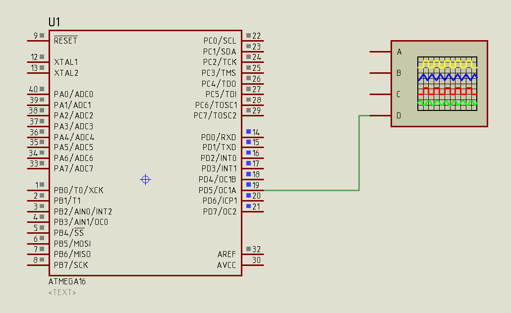

Results of circuit simulation in PROTEUS program
- Grid field 24x18 – consists of an image of vertical and horizontal white lines forming squares;
- Chess field – consists of white and black cells;
- Chess field with lines of clarity - vertical lines of clarity are introduced into the white cells;
- Brightness gradations – eight vertical stripes with a stepwise decrease in brightness from white to black;
- Red field;
- Green field;
- Blue field;
- White field;
- White field with clear lines;
- Horizontal color stripes – red, green, blue, turquoise;
- A universal test table, which includes elements of all of the above images, allows you to comprehensively evaluate the quality of the TV setup.


- text field of 17 lines;
- 8x6 mesh;
- mesh 12x9;
- small chess field 8x6;
- large chess field 2x2;
- white field.
- clock frequency - 12 MHz;
- supply voltage 3 - 5 V;
- current consumption in operating mode:
- at a supply voltage of 3V - about 5mA;
- at a supply voltage of 5V - about 12mA;
- frame rate - 50 Hz;
- number of lines per frame - 625
- 0 V - synchronization level;
- 0.3 V - black level;
- 0.7 V - gray level;
- 1 V - white level
3V - R5=456Ohm and R6=228Ohm
3.5V – R5=571Ohm and R6=285Ohm
4V – R5=684Ohm and R6=342Ohm
4.5V – R5=802Ohm and R6=401Ohm
5V - R5=900Ohm and R6=450Ohm
Estimated values are shown here. In reality, you can install resistors from the standard range, for example for 5V - 910 Ohm and 470 Ohm, and for 3V - 470 Ohm and 240 Ohm.